Michael does a good job designing stuff. This signal driver
he designed can drive any standard three aspect color light
signal, B&O CPL, or Pennsy PL. He has these drivers installed
in a rather large private HO pike, and has experienced very few problems
with them since installing them in 2000.
Signal Driver Overview
This board is intended for use with model
signal systems using a common anode system of 3 color LEDs in each head or in
the case of PRR Position Light (PL) 3 series LEDs in each aspect. It also has
the ability to drive one other LED, such as the single red LED in another head
on an absolute signal or the qualifier in B&O Color Position Light (CPL)
signals. The circuit is designed to permit each more restrictive signal
indication to override any more permissive indication. The default aspect is Clear.
Being designed for a standard single head, three aspect color light signal, this
driver circuit WILL NOT work with:
-- A B&O style CPL signal with more than one marker lamp,
-- A Pennsy style PL signal with all the options,
-- Or either a two or three head color light installation.
Common anode means the display LEDs all get connected to the +Vcc buss, and the
driving circuit completes the circuit to ground to light the LED.
Following 100 year old technology terms from the tube days (valve in the U.K.), the
anode of a tube, or LED in our case, gets connected to the plus side of the
power supply, and the cathode gets connected to the negative side. I
realize that most people reading this page may already know this
information, but for those of you who have not spent your whole
career playing with electronics, you may not know :-) :-)
If you have any questions, feel free to shoot me an email, but keep in mind, I
didn't design the circuit, and Michael can no longer be reached.
Mechanical Specifications
Here are the details for the PCBs Michael designed. You are of course,
free to design whatever you want, especially since I do not have access to any
of the files Michael used to create the PCB (Printed Circuit Board, AKA, PC
Board or just simply, PCB).
This board is made out of fiberglass reinforced resin, 0.062" thick, approximately 1/16".
Overall size, without connectors is 1.08" x 3.20".
The board has a black soldermask and white silk-screened legend/mask.
Edge card fingers are on 0.1" centers and intended for use with Sullins EZC10DREH or
equivalent connector.
Outputs to the LEDs on the signal mast are on a 5 contact Waldom/Molex
KK type connector with 0.1" centers. All exposed pads and edge card connections
are plated with tin/lead.
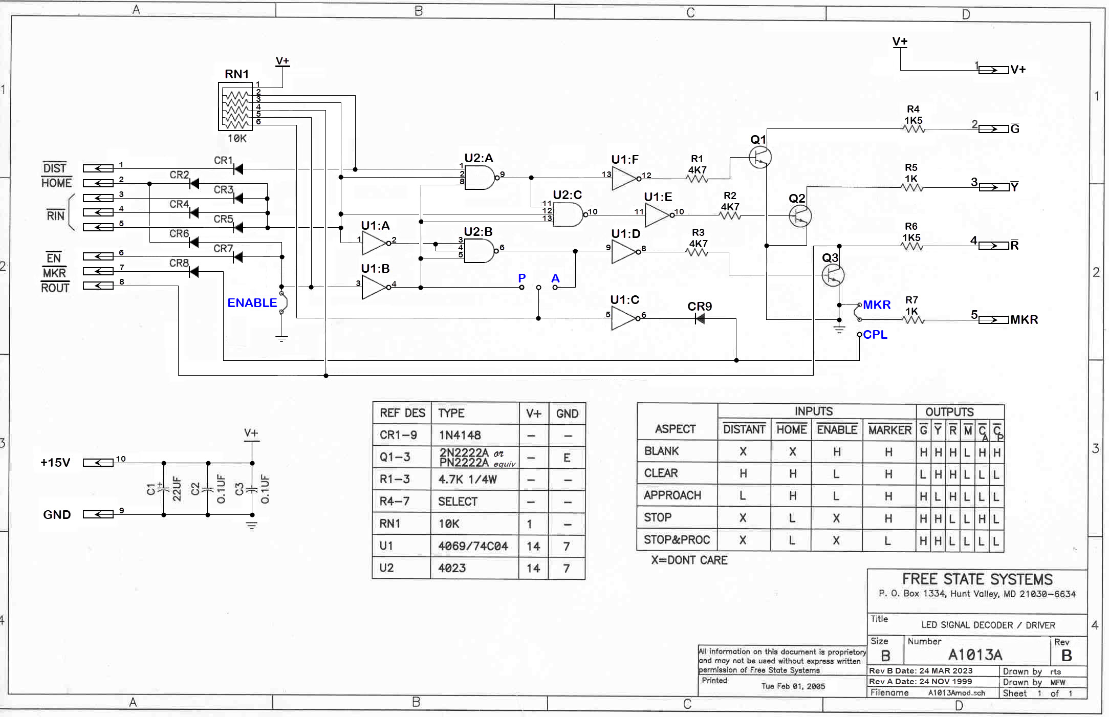
Circuit Description
This board is designed to operate from a 12 volt regulated power supply.
THIS IS IMPORTANT!:
All inputs are active low - that is, a "low" going signal
(or connection to ground) will activate the function. Diode isolation is
provided to allow multiple devices to be connected to the same electrical signal
without interference. Pull up resistors of 10K ohms are provided on the board to
insure unconnected inputs will be in a known state: off or non-activated.
All logic devices are 4000 series or 74C series CMOS.
An enable input is provided to allow approach lighting of the signal. Grounding
the \EN input on pin 6 will turn the LEDs on to display the selected indication. If
approach lighting is not desired, the enable jumper on the board should
be installed. This will keep the signals lit all the time.
The red,
yellow, and green
LED outputs are open collector transistors capable of driving up to 500 mA each
at 40 volts with an external power source with the proper selection of series
resistor. Pin 1 on the connector, is typically used to provide power to the
signal head. Normal operation is to select resistor values to match the
intensity of each color LED. Nominal values are installed to match many common
LEDs.
The marker is connected directly to ground
when the jumper is installed in the MKR position. The enable jumper should also
be installed when using this option. When in the CPL position, it is driven by
the output of the CD4069UB and is limited to a total of 3.5 mA divided between
the LED output and the \MKR output pin. The CPL output can be selected for
absolute or permissive operation. In the absolute mode, the marker is blanked
when the main head is displaying a red stop signal. The permissive mode allows
the marker to remain lit. In either mode, the marker is blanked when the signal
is not enabled unless the home input is low.
Installation and Operation
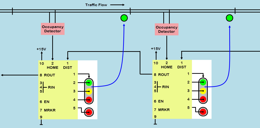
Here are the output connections for the signal head, these appear on the right side of the schematic:
-- Pin 1: A 12 volt supply is furnished for common anode signal heads.
-- Pin 2: Green.
-- Pin 3: Yellow.
-- Pin 4: Red.
-- Pin 5: For a CPL qualifier light or fixed red signal head.
Here are the input pins (except for pin 8) on the left side of the drawing:
-- Pin 1: \DIST - usually connected to the \Rout line of the next signal, or the current detector protecting the following
block. This will cause the signal to display a yellow approach indication whenever the next block is occupied.
-- Pin 2: \HOME - connected to the output of the detection circuit of the block protected.
-- Pin 3: \RIN - one of three, can be used to force a red stop indication whenever they are low.
-- Pin 4: \RIN.
-- Pin 5: \RIN.
Note 1: Note that these inputs will not force the display to be enabled like the \HOME input.
Note 2: These inputs can be connected to anything that will force a red display,
regardless of the track condition of the block ahead,
like a turnout set against the direction of travel or optical detectors at the ends of the block.
-- Pin 6: Can be jumpered to GROUND if this signal does not require approach lighting (or the enable jumper on the board can be installed).
-- Pin 7: Extra input to illuminate a 4th LED if so provided on the mast, will NOT override input conditions at pins 1 or 2.
-- Pin 8: /ROUT - same pin as in 4 above for an active red signal, active low.
-- Pin 9: Signal system GROUND.
-- Pin 10: +15VDC feed for the PCB electronics.
With no signal at either pins 1 or 2, the signal will display a GREEN indication.
To force a RED indication immediately, from say a switch contact, use a
LOW input on pin 3, 4, or 5. These pins are tied high.
The output on pin 5, the MKR output, does not have an output transistor driving the output.
Can't say for sure why he designed it this way. The only thing I can think of, is that
the R/Y/G outputs, if used for a CPL signal with three LEDs for each aspect, would exceed the
output capability of a single CMOS output - so a transistor is used to allow for
a larger current draw. The single MKR output, if used on a CPL signal, would
only be lighting a single white LED.
On-Board Jumpers
There are three jumpers on the board. I don't know why, but Michael did not go into the jumper functions
in HIS original circuit operation description, he forgot it completely.
So, 20 years later, I'm sitting here trying to figure out what is going on,
and why he might have designed these jumpers in this fashion. Here goes:
ENABLE:
- Placing a permanent jumper in this position will keep the signal lit at all times.
- Otherwise, a low input on pin 6 is needed to light the LEDs.
- An input on pin 2, HOME (which will give a red aspect), will do the same thing if the signal is not enabled and the LEDs are dark.
MRKR/CPL:
Assuming an LED is attached to this output: • IF the jumper is in the MKR position:
- Regardless of anything else going on with this circuit,
the LED will be lit as long as there is power, EVEN tho the signal head is dark! Careful using
this output, because NOTHING can control the MKR LED if connected here.!!!
• If the jumper is in the CPL position:
- The LED will light up when pin 7 (MKR) is grounded or goes low, regardless of any input or anything
else controlling the signal. -- If the "A/P" jumper is left open, the LED will be on all the time.
-- If the "A/P" jumper is in the "P" position:
---- And the ENABLE jumper is in place, the LED will be lit.
---- If the ENABLE jumper is NOT installed, and either the EN or HOME inputs go low, the LED will turn on.
-- If the "A/P" jumper is in the "A" position, the MKR output will be opposite of the RED output,
because there is no inverter transistor in the signal path,
---- Or, the LED will be on if a low is at the MKR input on pin 7.
A/P:
This gets messy, yuk. And..... the center pin between the "A" and the "P" is NOT labeled
- If no jumper is installed here, the input to U1C will be high, producing a low at the CPL jumper position,
and, if the MKR/CPL jumper is in the CPL position with an LED attached, the LED will light up.
- If strapped to the "A" position:
-- It will follow whatever the HOME input/RED LED is doing
but OPPOSITE, in other words, if the RED LED is on, the MKR LED
will be off. (That's an easy one to follow, because U1 is a hex inverter)
- If strapped to the "P" position:
-- The level at the CPL jumper position (and the MKR output) will be the same
as the EN input. Therefore, the LED will be on when ENABLE is low.
Remember this signal driver is using ACTIVE LOW logic, which makes it a little harder to follow along! (Yea, I hate it too :-)
There may be other conditions, but those are it after a quick examination, phew, I'm glad that's over. LOL
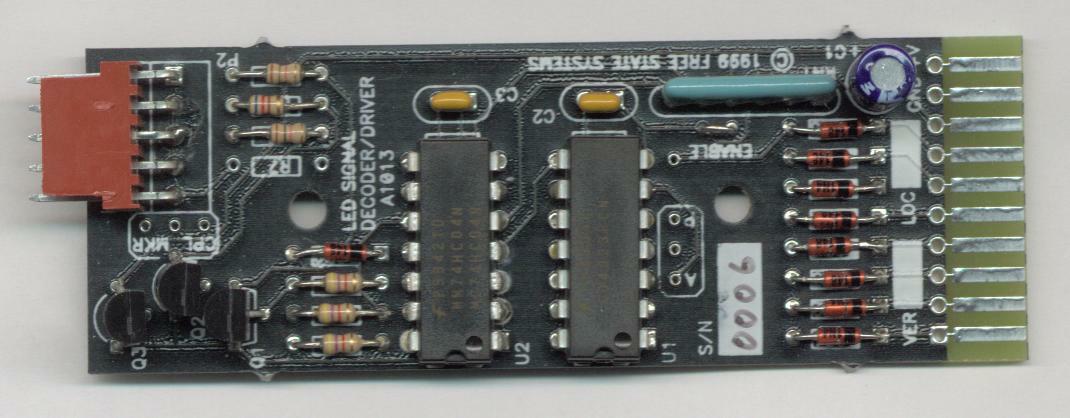
Below is a photograph of the circuit board, and below that is the schematic.
Output connections to the signal are on the right, input connections are on the left.
For additional info on this signal driver, email Michael at:
freestatesystems1@comcast..net
Sorry, as of the fall of 2025, I have not been able to get a hold of Michael
by either phone or email. I fear that we may have "lost him", because
about 10 years ago, he had a stroke which left him in poor condition.
If we have lost him, RIP my buddy, we had some good experiences over the past 55
years starting with EIL
Instruments in 1972!.....
Here is a basic connection diagram for two blocks:
Disclaimers:
New format 10/26/23: Please check out my disclaimer page for my standard
dribble and contact info here